What is PCB?
PCB stands for Printed Circuit Board, and it is a medium to connect electronic components in a controlled manner.
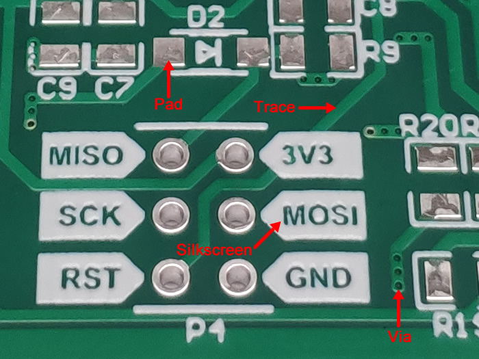
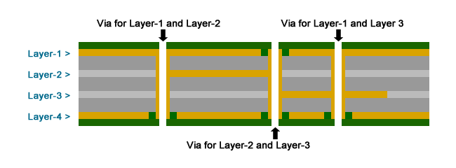
A PCB has laminated sandwich structure and there is insulating layer between condutive layers. Each conductive layer is etched to specific patterm (trace, pad etc.) that serves as conductive wires on the plane, and different conductive layer can get connected at some points (which is called via) to implement more complex wiring.
A PCB may have multiple conductive layers, but electrical components can only be soldered on top or bottom conduntive layers. Below is an example of 4-layer PCB (meaning it has 4 conductive layers), and it demonstrate how vias connect the traces in different layer.
The conductive layers are usually made of copper. There are different kinds of insulating substrate meterials for PCB, but FR-4 glass epoxy is the most common one. If the component needs extra cooling, aluminum substrate (clad with thermally conductive thin dielectric) may be used.
Only the pads that will get soldered with components will be exposed on top or bottom surface, other areas will be covered with solder mask (also known as solder resist). The most common color for solder mask is green, but there are also other colors like blue, red, yellow, purple, black, white etc.
Silkscreen (also known as silk or legend) is printed on top or bottom surface of PCB. It provides information like component designator, product LOGO, instructive guide for assembling, testing or usage of the PCB. The silkscreen is usually in white color, but there are also other colors available.