How to export gerber files from Kicad?
It is recommended to export the PCB design to gerber files, and then us them for manufacturing.
In this tutorial you will learn how to export your PCB design in Kicad to gerber files.
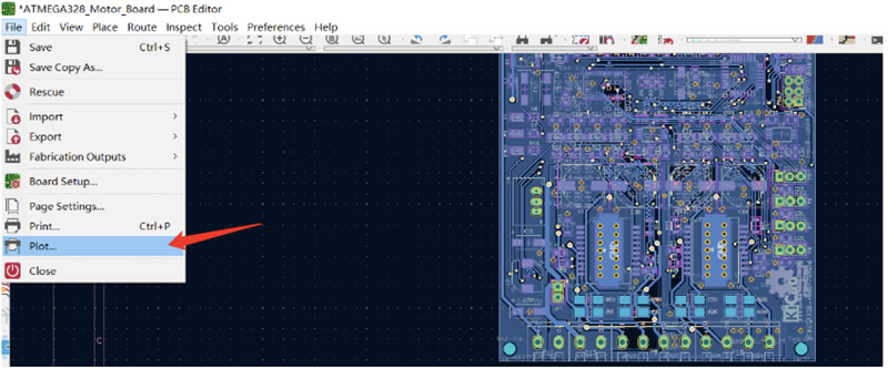
After loading the PCB design, choose menu File->Plot…:
In the pop-up window, specify the output directory for saving the gerber files, and also choose the layer to be included.
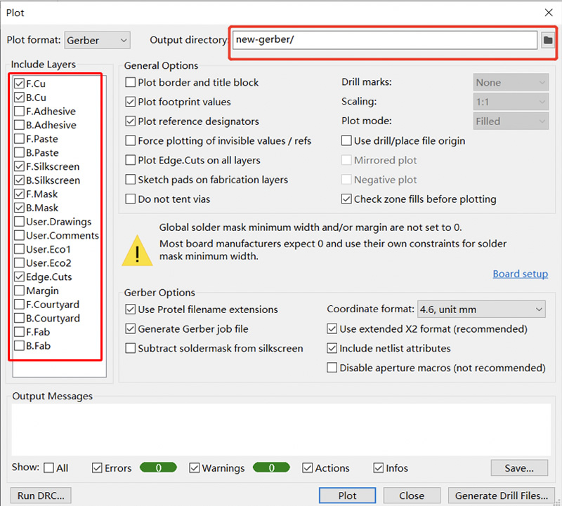
The “F.” in layer name indicates the layer is on the front, while the “B.” in layer name indicates the layer is on the back. The copper layers have “Cu” in their layer names, while the solder mask layers have “Mask” in their names, and silk screen layers have “Silkscreen” in their names accordingly. The “Edge.Cuts” layer is the one who defines the board shape.
Click the “Plot” button at the bottom to output the gerber files. After that you can click the “Generate Dril Files…” button at the bottom, which will bring up a window that allows you to specify the parameters for drill file.
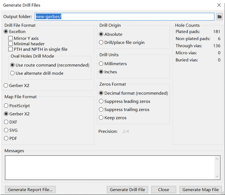
Click the “Generate Drill File” button at the bottom to output the drill file.
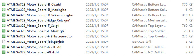
Now the gerber files are ready. You can pack them as a ZIP file and submit in our inquiry page for PCB preview and price estimation.